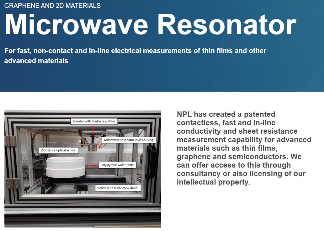
2D scanner for metal deposition on silicon wafer
In 2018, I have led the development of a demonstrator of a microwave resonator for our quantum division. I have chaired the meetings and led our team of three engineers to deliver 2D scanner to check the metal deposition on silicone wafers up to 200mm (a photo of the apparatus can be found here: https://www.npl.co.uk/products-services/graphene-2d-materials/microwave-resonator). The team was also assisted by a project manager.
The main constraints of the project were the limited time and limited budget to deliver one unit. The project required to familiarise with the sensor patented by NPL and propose a way to integrate it on a home-made gantry. The initial requirement from the internal customer was to develop a demonstrator for a typical application such as assessing copper mesh, thin flexible films, silicone wafer, metallic powder or else. After proposing different concepts, my team decided to focus on the silicone wafer scanner. Due to the small budget, I proposed three different level of technology to build the gantry system: the modification of 3D printer, the in-house build of a gantry made of off-the-shelf linear actuators, purchase the whole motion system, and integrate it with other components. We kept the second solution, and I produced the whole mechanical design and sourced the main components, including the electronic driver, and I familiarised myself with its programming language to support our software engineer.
The main frame is composed of aluminum extrusions, and to reduce the costs, I involved two of our apprentices and an intern. I have ordered raw material, produced a detailed drawing with a cut list and asked them to build the enclosure. During this period, the lab where they were working closed temporarily and they relocated without my knowledge in another lab with low light level, working on the floor and without producing a risk assessment. I raised this concern to my manager, and I could relocate them in a proper place where they could complete the work safely. Another issue arises when they delivered the enclosure with wrong dimensions, so that the door could not fit. This event frustrated me, as the time was pressing. I seek the help from my line manager to understand if I was wrong in my communication. I was reassured by him this was common with junior staff who need closer monitoring of their activities. I improved the situation by engaging more with them and find a way to keep working without wasting some of the work they have already done.
The demonstrator was delivered as promised, I am thankful to my two colleagues, who helped with drawing edition, wiring, software writing, debating the various technological options we got. Along the development of this instrument, I engaged with the principal scientist to confirm some design choices, and later to support him troubleshooting the apparatus.

